“During the several months of the contract, I felt incredibly grateful for what you did for Finisar, and much more deeply realized just how unique the service you provide is!”.–Bob Herrick, Ph.D.
3 ESD Class 0 Success Stories | ESD Myths, Latency & Success Stories | EOS Misdiagnosis & Success Story | Economic Benefits | Testimonials
EOS vs. ESD Misdiagnosis and Success Story:
Charged-Board Events: A Growing Industry Concern!
By
Ted Dangelmayer & Terry Welsher
Dangelmayer Associates, L.L.C., 14 Butternut Lane, Gloucester, MA 01930 USA
tel: 978 282 8888, e-mail ted@dangelmayer.com
Andrew Olney
Analog Devices, Inc., 804 Woburn Street, M/S 424, Wilmington, MA 01887 USA
tel.: 781-937-2362, fax: 781-937-2012, e-mail: andrew.olney@analog.com
A common myth persists today that devices mounted onto printed-circuit boards are significantly less vulnerable to ESD. However, it has long been known that ICs and other ESD-sensitive components remain at risk during board assembly and subsequent handling and installation. The myth has been compounded by the fact that most ESD testing and characterization of these components has been done on stand-alone parts. Further, IC failure analysis data, which is based on knowledge of failure signatures seen in standard HBM and CDM tests, has caused many to conclude that ESD failures are relatively rare when compared to other electrical failures commonly classified as electrical overstress (EOS).
Recent data and experience reported by several companies and laboratories now indicate that many failures previously classified as EOS are instead the result of ESD failures due to Charged Board Events (CBE) or Cable Discharge Events (CDE). As their names imply, a CBE discharge occurs when a charged circuit board is suddenly discharged, while a CDE discharge occurs when a charged cable is suddenly discharged. While this article focuses on CBE ESD failures, some of the analysis is also applicable to CDE ESD failures; both types of discharges can result in very high energy events that severely damage ICs and other components.
A Charged Board stores much more energy than a device (IC) because its capacitance is many times larger. In fact, the charge (energy) transferred in the event is so large that it can cause EOS-like failures to the components on the board. Figure 1 illustrates considerably more extensive damage resulting from the CBE than CDM of the component separately. The vast majority of FA experts would incorrectly diagnose the CBE damage as EOS.
")
Charged Board Event: Field Returns
The following investigation provides an example of ICs that are robust to ESD at the component-level but were nonetheless damaged by ESD at the board-level. The damage was simulated via Field-Induced Charged Board Event (FICBE) testing using a conventional CDM test system. For a given charge voltage, the CBE discharge waveforms had much higher peak currents than the corresponding CDM discharge waveforms. Thus, the CBE damage was more severe than the CDM damage. In some cases, the CBE damage was so severe that it could easily be mistaken for EOS damage. The susceptibility of a given IC to CBE damage is a complex function of variables including the IC on-chip protection network; the IC package design; the size of the power planes on the PCB; and the number of power supply pins on the IC tied to the power planes.
During system-level production testing and field application, a customer had a several hundred PPM failure rate on a four-level-metal, deep-submicron CMOS DSP packaged in a 28 mm x 28 mm, 208-lead Plastic Quad Flat Pack (MQFP). The failure modes varied, but typically involved functional failures within a small block of circuitry within the DSP.
The DSP was located near a corner of the PCB above relatively large copper ground planes in both the top and bottom layers of the PCB. All the components were on one side of the customer’s four-layer PCB. The top and bottom ground planes were interconnected by numerous plated through-holes. The 35 GND pins on the DSP package were tied to the interconnected copper ground planes, while the 33 Vdd pins were tied to an internal copper Vdd power plane. The other internal PCB layer was used for routing I/O signals.
FICBE testing was conducted using a KeyTek Verifier Robotic CDM test system. To assist simulating the failures, the customer provided numerous PCBs. Since the complete customer PCB was larger than the 127 mm (5”) field charging plate, the PCBs were cut-down in size. However, the ground plane under the DSP was kept fully intact. (Note: More complete details on the customer’s PCB design are not provided since this information is proprietary.) Since full electrical testing of the cut-down PCBs was not feasible, the DSP on each PCB was decapsulated to expose the die for visual inspection purposes. Initial high-magnification die inspection of the DSPs on the PCBs revealed no anomalies like those previously noted.
The FICBE test method for each customer PCB was as follows:
- The cut-down PCB was centered on the charging plate (see Figure 2). Fortunately, the PCB had no components on the bottom side, so it rested flat on the charging plate. In this configuration, the capacitance measured between the PCB ground planes and the charging plate was ˜420 pF, while the capacitance between the PCB Vdd plane and the charging plate was ˜460 pF.
- The charging plate was raised to +125V and then the ground plane was discharged at a test pad close to the edge of the PCB. Consistent with the methodology in ESDA STM5.3.1-1999, this was repeated two more times.
- High magnification optical die inspection was conducted to look for the onset of damage.
- The charging plate was brought to –125V and then the ground plane was discharged at the same PCB location. This was repeated two more times.
- High magnification die inspection was again conducted to look for the onset of damage.
- Consistent with the procedure in Steps 2-5, the ground plane on the same PCB was subjected to FICBE testing in 125V charge voltage increments until high-magnification optical inspection revealed damage.

DSP IC Failure Analysis:
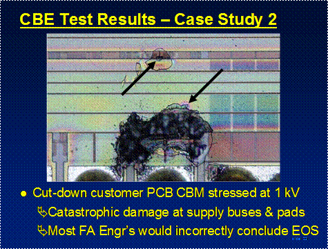
The damage resulting from a 1 kV stressing voltage is shown in figure 3. The resulting discharge waveforms are shown in figure 4. The CBE discharge current is approximately 9 amps while the CDM peak current of the device alone is under 4 amps. These stresses frequently exceed the design capabilities of IC’s. The damage is far more sever than typical of CDM device stress testing (JEDEC C101) and would be misdiagnosed by the vast majority of FA experts.
This work has resulted in the development of an uncommon FA expertise. It appears that approximately 50% of real-world “EOS” failures are actually ESD at the circuit board level (CBE) or at the system level (CDE).
This discovery is especially significant since the vast majority of FA reports indict EOS as the root cause when ESD is the true failure mechanism. These incorrect diagnostics trigger costly and ineffective corrective actions in manufacturing and in chip design. They also trigger dead-end investigations into test equipment and power supplies.

Conclusions
Misdiagnosis of EOS failures is a widespread and costly problem within the electronics industry. Where careful data has been collected, it has been demonstrated that approximately 50% of the so-call EOS failures are actually ESD at the board level (CBE) or system level (CDE).
These data suggest that failure analysts should give stronger consideration to these types of board-level and system-level ESD events before assigning an EOS diagnosis to the failure. This will support more effective root cause analysis and prevention of these failures. The discharge currents in many cases exceed the design capabilities of either IC’s or circuit boards. Thus, manufacturing and field ESD control methods become critically important and the primary line of defense.
Since the CBE is nearly the same mechanism as CDM, the factory and field control methods are similar to those for CDM. The diagnostics involve EMI ESD event detection and warrant a full understanding of the physics of CDM and ESD by induction.
Charged Board Event: Manufacturing
A separate experience illustrates how the CBE can take place in a manufacturing operation. Many printed wiring assemblies (circuit boards) include a cover or faceplate which provides a protective covering when the board is installed in a system (figure 5). To keep material costs down, they are often made of insulating plastic.
In this case, the board was in production for more than a year without any indication of a significant problem. Suddenly, however, the removal rate of a certain linear CMOS part began to rise. The failure rate averaged 2.5% with rates as high as 40% on certain days. The device failures were observed after circuit board test and the observed electrical signature was excessive leakage current between two pins on the device. The leakage was high enough to cause the circuit board to fail its functional requirements.
These observations and subsequent Failure Modes and Effects Analysis (FMEA) pointed strongly to CBE ESD as the source of the problem. The production line had a well-designed ESD program known to be in compliance with the current best practices. Further, a careful analysis of the line produced no indication of why this particular part was failing at higher than normal levels.
Most significantly, the failing component was well designed with a charged-device model (CDM) withstand voltage of 1,500 volts.

While investigating changes in the design and materials, it was learned that the source of the plastic for the faceplate had changed around the time that the failure levels began to increase. Both the base resin and the molder had changed. It was then found that the electrostatic voltages on the faceplates were extremely high, with 10 kV being typical, and that these voltages persisted for days or weeks. Laboratory investigations then showed that the faceplates from the new source tended to charge to levels about five times higher than the previous ones and that the charge retention was much longer as well.
For reasons that will become clear in this discussion, the board/device level failure mode analysis was difficult. Eventually, it was demonstrated that the exact failure as was observed in the factory could be produced by tribocharging the faceplate and then touching (grounding) the circuit board in a particular way. This was a classic example of a field-induced CBE (CDM) failure. Initial investigations into the failure mechanism of the circuit boards indicate that the pin (21 or 22) which failed in the factory (figure 5) was never physically touched during testing and/or handling of the circuit board. This was surprising because the CBE/CDM failure of a pin requires that the pin be grounded. Thus, further studies were conducted in the laboratory which confirmed that the pin 21-22 leakage current could be produced by touching a pin on a transformer mounted near the faceplate.
Pins 21 and 22 were connected by a low resistance bus on the PCB to pin 36 of the CMOS device (Figure 5). Thus, the pin which exhibited the failure was different than the pin stressed. This is not unusual for CDM events. However, this is seldom observed in routine qualification of devices because post-stress testing of the device is usually only done after all pins have been stressed. Therefore, it is important in FMEA investigations to stress the device in a manner which resembles as closely as possible the actual sequence of real-world events in order to confirm the failure mechanism.
The next step was to understand how the charging and discharging events were occurring in the factory. With the aid of ESD event detectors, the discharges were found to be occurring during the testing of the circuit board. The entire scenario is represented schematically in Figure 5. When the circuit board with its charged faceplate was placed in the “bed-of-nails” tester, the first test probe to touch the board touched a pin on the transformer near the charged faceplate. The transformer pin was about 1/2-inch from the charged faceplate. Because the voltages on the faceplates were very high, it is easy to imagine that the effective induced voltage as seen by the board resulted in a discharge current that exceeded the device capability. As noted above, these discharge currents often far exceed the design capability of either the components or circuit boards. Thus, sound CBE manufacturing practices are both essential and the baseline of defense. It is not longer possible to just rely on designed-in protection.
References:
- Olney, Andrew et al., “Real-World Charged Board Model ESD Failures,” EOS/ESD Symposium, 2003.
- Dangelmayer, G. Theodore, “ESD Program Management,” 2nd Edition, Kluwer Academic Publishers, 1999.
- T. Dangelmayer, “ESD Myths and the Latency Controversy,” Compliance Engineering, Spring 2002.
- R. Peirce, “The Most Common Causes of ESD Damage,” Evaluation Engineering, November 2002.
- K. Banerjee, D-Y Kim, A. Amerasekera, C. Hu, S. S. Wong and K. Goodson, “Microanalysis of VLSI Interconnect Failure Modes Under Short-Pulse Stress Conditions,” IEEE International Reliability Physics Symposium, pp. 283-288, 2000.
- ESD Association Standard Test Method STM5.3.1-1999, Electrostatic Discharge (ESD) Sensitivity Testing – Charged Device Model (CDM) – Component Level, ESD Association, 1999.