Full Range of ESD & EOS Consulting Services: Training, Auditing, CDM, CBE, CDE, Class 0, Cleanrooms, S20.20 Programs
No Product Sales!
Our Services » ESD/EOS » Charged Board Event
Best Practices | Audits | Training | CBE | CLASS O | S20.20 | Documents | Testimonials
CBE | CBE Technical Assessment | Root Cause Analysis | EOS Seminar Outline
EOS vs. ESD Misdiagnosis:
Charged-Board Events: A Growing Industry Concern!
“50% of EOS failures are actually caused by ESD at the Circuit Board level!” Andrew Olney, Quality Director, Analog Devices
“The vast majority of FA experts would incorrectly diagnose the CBE damage as EOS.”Andrew Olney, Quality Director, Analog Devices
A common myth persists today that devices mounted onto printed-circuit boards are significantly less vulnerable to ESD However, it has long been known that ICs and other ESD-sensitive components remain at risk during board assembly, handling and installation. The myth has been compounded by the fact that most ESD testing and characterization of these components has been done on stand-alone parts. Further, IC failure analysis data, which is based on knowledge of failure signatures seen in standard HBM and CDM tests, has caused many to conclude that ESD failures are relatively rare when compared to other electrical failures commonly classified as electrical overstress (EOS). Recent data and experience reported by several companies and laboratories now indicate that many failures previously classified as EOS are instead the result of ESD failures due to Charged Board Events (CBE).
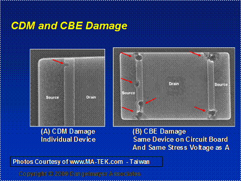
A Charged Board stores much more energy than a device (IC) because its capacitance is many times larger. In fact, the charge (energy) transferred in the event is so large that it can cause EOS-like failures to the components on the board. Figure 1 illustrates considerably more extensive damage resulting from the CBE than CDM of the component separately. “The vast majority of FA experts would incorrectly diagnose the CBE damage as EOS.” – Andrew Olney, Analog Devices
Synopsis:
Case Study #2: Olney, Andrew et al., “Real-World Charged Board Model ESD Failures,” EOS/ESD Symposium, 2003, http://www.analog.com/static/imported-files/quality_assurance/eos_esd_03_paper_1.pdf
Background
Case Study 2 – DSP IC
- ~200 PPM customer PCB failure rate
- One DSP IC per board
- Deep-submicron CMOS; 4-level metal
- 208-lead Plastic Quad Flat Pack
- 35 GND pins & 33 Vdd pins
- DSP operated within Absolute Max. Ratings
- DSP located at corner of PCB
- Failure Mode: typically functional failures
- Could not simulate this via HBM or CDM
Stress Test Method:
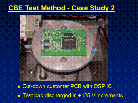
In order to simulate the event which occurred in the hands of the customer, a circuit board containing the DSP IC was cut to fit on the charging chuck of a commercial CDM tester. (figure 2). The circuit board is separated from the chuck by a thin sheet of Mylar film. The chuck is then biased to the desired voltage which results in a static field that charges the board similarly to real life exposure to induction. The discharge is created by contacting the desired pin of the DSP IC with the discharge head of the CDM tester and, thus, completing a CBE discharge by ESD induction. The stressing voltage and discharge were then increased in 125 volt increments.
DSP IC Failure Analysis:
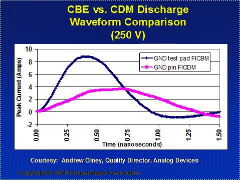
The damage resulting from a 1 kV stressing voltage is shown in figure 3. The resulting discharge wave forms are shown in figure 4. The CBE discharge current is approximately 9 amps while the CDM peak current of the device alone is under 4 amps. These stresses frequently exceed the design capabilities of IC’s. The damage is far more sever than typical of CDM device stress testing (JEDEC C101) and would be misdiagnosed by the vast majority of FA experts.
Analog Devices has developed an uncommon FA expertise in this area and determined that approximately 50% of their EOS failures are actually ESD at the circuit board level or CBE.
This discovery is especially significant since the vast majority of FA reports indict EOS as the root cause when ESD (CBE) is the true failure mechanism. These incorrect diagnostics trigger costly and ineffective corrective actions in manufacturing and in chip design. They also trigger dead-end investigations into test equipment and system-level environments.

Conclusion
Misdiagnosis of EOS failures is a wide spread and costly problem within the electronics industry. Where careful data has been collected, it has been demonstrated that approximately 50% of the so–call EOS failures are actually ESD at the board level (CBE).
These data suggest that failure analysts should give stronger consideration to these types of board-level events before assigning an EOS diagnosis to the failure. This will support more effective root cause analysis and prevention of these failures. The discharge currents in many cases exceed the design capabilities of either IC’s or circuit boards. Thus, manufacturing and field ESD control methods become critically important and the primary line of defense.
Since the CBE is nearly the same mechanism as CDM, the factory and field control methods are CDM in nature. The diagnostics involve EMI ESD event detection and warrant a full understanding of the physics of CDM and ESD by induction.
Case Study:
ESD (Field-Induced CDM) Caused by Charged Plastic Faceplate – Book “ESD PROGRAM MANAGEMENT” by Ted Dangelmayer
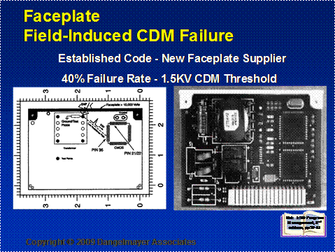
A recent experience in one factory illustrates how the CBE can take place in a manufacturing operation. Many printed wiring assemblies (circuit boards) include a cover or faceplate which provides a protective covering when the board is installed in a system (figure 5). To keep material costs down, they are often made of insulating plastic.
In this case, the board was in production for more than a year without any indication of a significant problem. Suddenly, however, the removal rate of a certain linear CMOS part began to rise. The failure rate averaged 2.5 percent with rates as high as 40 percent on certain days. The device failures were observed after circuit board test and the observed electrical signature was excessive leakage current between two pins on the device. The leakage was high enough to cause the circuit board to fail its functional requirements.
These observations and subsequent FMA pointed strongly to CBE ESD as the source of the problem. The production line had a well-designed ESD program known to be in compliance with the current best practices. Further, a careful analysis of the line produced no indication of why this particular part was failing at higher than normal levels.
Most significantly, the failing component was well designed with a charged-device model (CDM) withstand voltage of 1,500 volts.
While investigating changes in the design and materials, it was learned that the source of the plastic for the faceplate had changed around the time that the failure levels began to increase. Both the base resin and the molder had changed. It was then found that the electrostatic voltages on the faceplates were extremely high, with 10 kV being typical, and that these voltages persisted for days or weeks. Laboratory investigations then showed that the faceplates from the new source tended to charge to levels about five times higher than the previous ones and that the charge retention was much longer as well.
For reasons that will become clear in this discussion, the board/device level failure mode analysis was difficult. Eventually, it was demonstrated that the exact failure as was observed in the factory could be produced by tribocharging the faceplate and then touching (grounding) the circuit board in a particular way. This was a classic example of a field-induced CBE (CDM) failure. Initial investigations into the failure mechanism of the circuit boards indicate that the pin (21 or 22) which failed in the factory (figure 5) was never physically touched during testing and/or handling of the circuit board. This was surprising because the CBE/CDM failure of a pin requires that the pin be grounded. Thus, further studies were conducted in the laboratory which confirmed that the pin 21-22 leakage current could be produced by touching a pin on a transformer mounted near the faceplate.
This pin was connected by a low resistance bus on the PWB to pin 36 of the CMOS device (Figure 5). Thus, the pin which exhibited the failure was different than the pin stressed. This is not unusual for CDM events. However, this is seldom observed in routine qualification of devices because after-stress testing of the device is usually only done after all pins have been stressed. Therefore, it is important in FMA investigations to stress the device in a manner which resembles as closely as possible the actual sequence of events in order to confirm the failure mechanism.
The next step was to understand how the charging and discharging events were occurring in the factory. With the aid of ESD event detectors the discharges were found to be occurring during the testing of the circuit board. The entire scenario is represented schematically in Figure 5. When the circuit board with its charged faceplate was placed in the “bed-of-nails” tester, the first test probe to touch the board touched a pin on the transformer near the charged faceplate. The transformer pin was about 1/2-inch from the charged faceplate. Because the voltages on the faceplates were very high, it is easy to imagine that the effective induced voltage as seen by the board resulted in a discharge current that exceeded the device capability. As noted above, these discharge currents often far exceed the design capability of either the components or circuit boards. Thus, sound CBE manufacturing practices are both essential and the baseline of defense. It is not longer possible to rely on designed-in protection.

