“During the several months of the contract, I felt incredibly grateful for what you did for Finisar, and much more deeply realized just how unique the service you provide is!”.–Bob Herrick, Ph.D.
3 ESD Class 0 Success Stories | ESD Myths, Latency & Success Stories | EOS Misdiagnosis & Success Story | Economic Benefits | Testimonials
Three ESD Class 0 Success Stories
The following Class 0 (see definition below) case studies illustrate the complexity and customization required to successfully produce products utilizing these ultra-sensitive devices. They also form the basis of a third party qualification for Class 0 manufacturing operations by the ESD Journal.
It should be noted the term Class 0 has not been defined for manufacturing applications by any industry standard. We have found that manufacturing failure rates escalate exponentially for devices with ESD withstand voltages below 250 volts for either HBM or CDM. MM is intentionally omitted from this definition since it is largely redundant to HBM. It is also vitally important for the manufacturing process to have a well-defined trigger for risk assessments of these ultra-sensitive components. These risk assessments involve verification of manufacturing process capability as well as for any risks that may be passed on to customers. In some instances, risk assessments have resulted in the redesign of components to improve the ESD performance. Thus, we propose to define a Class 0 area for ESD manufacturing as one that includes components that have withstand voltages below 250 volts for either HBM or CDM.
It has become clear that customized manufacturing requirements for Class 0 products are essential. It is unlikely that any standards body will be able to develop a cookbook process in the foreseeable future. The variables are far too great for standardization. Hence the ESD Journal has developed a Seal of Approval.
ESD Journal Class 0 Manufacturing Seal of Approval
The ESD Journal www.esdjournal.com has taken the initiative to develop a Class 0 ESD Journal Seal of Approval for customized manufacturing operations dealing with these ultra-sensitive devices. The qualification is based on peer review of application appropriate customization for Class 0. It must be clearly demonstrated that the petitioning company has sufficient advanced technical expertise as well as documented Class 0 procedures, yield success and exceptional compliance to procedure.
Two companies have achieved this outstanding level of recognition, Harold Datanetics Limited, China for their Class 0 Tape Head product manufacturing and BAE Systems - Nashua, NH - USA for Class 0 Manufacturing Excellence. BAE Systems has also completed their bi-annual requalification. Additional companies are working diligently for the same recognition.
Class 0 Case Study #1: Production Stoppage
This Class 0 case Study took place during ramp up of a Billion dollar product line and at a time when the advanced auditing techniques such as ESD event detection and current probe measurements were not being practiced. The production line was virtually shut down due to high failure rates. Severe yield loses coincided with the Introduction of an N-type metal oxide semiconductor (NMOS) device that had an ESD withstand voltage of 20 volts for both HBM and CDM. Major problems were encountered during device fabrication as well as during the assembly of the printed wiring board (PWB).
These low thresholds were the result of the lack of protection circuitry on the high-speed pins of the device. The designers presumed that any such circuitry would prevent the device from performing its intended function. They were ultimately able to redesign the device and attain 1000 volt withstand voltages without compromising system performance. However, it was not in time to avert the following production crisis.
PWB Assembly
PWB assembly failure rates (Figure 1) were fluctuating between 10 and 30 percent and some lots were 100-percent defective. Production was at a virtual standstill.
The cost implications of their continued failure were very high and were jeopardizing the entire product line. A detailed failure analysis investigation revealed that virtually all of the failures were ESD-induced.
A technical assessment of the manufacturing line was undertaken, and an action plan compiled based on conventional wisdom at the time. Because of the extreme seriousness of this situation, the weekly reports were channeled to high-level executives in the company.
Initially, many extraordinary handling precautions were instituted such as whole room ionization, bench ionizers, ESD garments, ESD chairs, constant wrist monitors, daily compliance verification etc. Even with nearly flawless compliance to procedure yields continued to fluctuate dramatically.
This problem was resolved with the introduction of a customized dissipative shunt referred to as a “top hat” (figure 2). This shunt consisted of molded static dissipative foam precisely contoured to contact each lead of the device while on the circuit board. The top hat was placed on top of the NMOS device immediately after it had been assembled to the PWB. This resulted in the leads of the device being electrically connected through the static dissipative foam and static potential differences minimized.
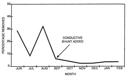
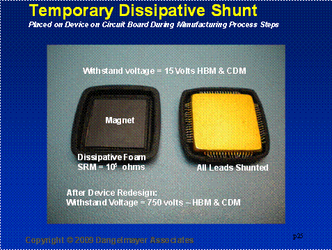
The board was then processed normally through the rest of the assembly line until it reached final test when the Top Hat had to be removed. This simple addition of a shunt to the device dramatically improved yields and resulted in failure rates of less than 2 percent.
The simplicity of this solution is particularly striking in contrast to more common alternatives that proved to be unsuccessful and costly. Thinking outside the box provided immediate resolution with minimal expense. The extraordinary measures of using a multitude of standard precautions proved to be overkill and ineffective. The solution described here introduces a simple shunt into a set of existing procedures. The incremental cost was merely $1,000 for a set of Top Hats. Yet the dollar savings realized on the production line reached $6.2 million per year for this one device on this one line and enabled a Billion dollar product line to ship on time. That is an impressive payback by any measure.
One additional benefit derived from this case was the impact that it had on the design community. Asked to justify a withstand voltage of 20 volts for the NMOS device involved in the project, designers responded by redesigning the device and raising the level of sensitivity to 750 volts HBM & CDM, a remarkable accomplishment. Some system level design changes were made to accommodate the new protection circuitry and maintain the system performance.
This case study makes it clear that ultrasensitive devices pose as significant threat to production lines that may result in lost production and lost sales. The financial implications are particularly unattractive when the cost of lost sales is added to the cost of lost materials.
As a direct result of the experience outlined in this case study, minimum design requirements were modified and a new set of handling requirements for Class 0 were established. It was apparent that a cookbook approach to establishing handling criteria for ultrasensitive devices would not work. For example, it is likely that some of the automated equipment used in the assembly process was causing the problem solved by the application of a top hat. Clearly, the extraordinary controls such as room ionization could not solve the problem. Adding a shunt was not only necessary but sufficient to protect the device at great economic benefit. In addition, the manufacturing line was able to continue to do operate as usual with minimal disruption.
In conclusion, a number of valuable lessons learned were derived from this experience that have lead to today’s advanced approaches for Class 0 sensitivities. Firstly, design transfer or new product introduction checklists must include ESD sensitivities followed by risk assessments for devices below 250 volts or redesign of the product to eliminate these ultra-sensitive components. It is also apparent that customized solutions are essential for cost effective mitigation of ESD failures. The advanced auditing techniques available today such as ESD event detection and current probe analysis enable scientific determination of optimal controls and counter measures. The final ingredient is technical expertise to conduct advanced measurements and to develop application appropriate remedies. These lessons learned helped to create a foundation for the following case studies as well as the creation of ESD Journal Class 0 Seal of Approval.
Class 0 Case Study #2: Harold Datanetics Limited, China
Background:
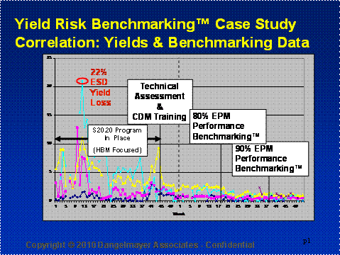
This case study took place in China at an MR Tape Head manufacturing site with Class 0 devices. ESD failures rates had previously been documented as high as 22%. (See Figure 3) Each data point on the trend lines is confirmed ESD damage and each colored line represents one product’s performance.
An HBM program had been in place for a number of years and concerted efforts to reduce the ESD yield losses had been unsuccessful. An ESD Consultancy was hired to not only to improve yields for current products but also to prepare for the next generation of heads that were expected to have sensitivities as low as 10 volts. The yields are now over 99.6% as shown in figure 1, including the next generation.
Baseline Technical Assessment
The first step to resolving the yield losses was to conduct a baseline technical assessment. A detailed analysis of each operation revealed minimal HBM compliance issues and the program was in good alignment with ANSI/ESD S20.20. However, numerous CDM compliance issues were noted that ultimately proved to be the root cause of the high yield losses. Advanced auditing techniques were applied that included a variety of ESD event detectors and high-bandwidth current probes. More traditional measurement techniques such as electrostatic voltages were helpful but insufficient to detect the subtle sources of the losses. Event detection and current probe measurements have become essential tools for Class 0 applications.
These advanced techniques enabled the systematic modification of each manufacturing operation to be either ESD discharge event free or to exhibit events no larger than 1/10th that of the current failure threshold of the MR Heads.
Resolving CDM manufacturing issues required a two-pronged approach. (See Figure 4) Voltages on the product had to be reduced with the customary strategies of removing static generators, minimizing triboelectrification of the product, and the strategic ionization. Targeted application of ionizers reduced both purchase and maintenance costs. MR Head competitors had installed ionizers at every work station and, as a result, incurred substantial and unnecessary expenses.

The second of the CDM mitigation techniques involved controlling surface resistances, and thereby discharge currents, at the point of contact between the ESDS product and the various manufacturing tools and fixtures. With the aid of the advanced auditing equipment, each operation was modified to ensure discharge currents were invariably below preset limits. These modifications consisted largely of the substitution of static dissipative materials and special operating procedures. This approach greatly reduced the number of ionizers and was more effective than wide spread ionization.
Advanced CDM Training Workshop:
A multi-day workshop was conducted to elevate the customers understanding of CDM and the technically advanced measurement techniques. Ultimately, the customer must be able to fully understand Class 0 mitigation techniques and the measurement techniques. This training was reinforced with ongoing technical support for a full year that proved to be essential. At the end of the year, HDL staff was fully capable of dealing with the next generation of 10 volt sensitivities by themselves. This level of understanding is required to achieve the Class 0 Seal of Approval.
EPM Yield Risk Benchmarking™ and ESD Quality Metrics:
Throughout this process ESD Quality Metrics were used to track the improvements.( See figures 5; 6; 7; 8 & 9) EPM Yield Risk Benchmarking™ and meaningful quality metrics are an organizational manufacturing necessity. This enables management to set measurable goals and objectives and to efficiently monitor progress.
This benchmarking method is an accurate means of quantifying the performance of an ESD program and there is a direct correlation to personnel compliance with ESD procedures. It has been successfully applied to hundreds of ESD programs and invariably producing robust long term program stability. Even when conducted over the phone, the EPM Yield Risk Benchmarking™ accurately (within 90%) reflects compliance to procedure and to corresponding yield improvements.
Each bar in Figure 3 represents the Benchmarking score of a single manufacturing location. As noted, the MR Head company in this case study improved from a score of 36% to 94% in one year and realized a corresponding yield improvement. This data is also represented in Figure 4. Note that a program can be optimized and, thus, avoid overkill with unnecessary and expensive solutions.
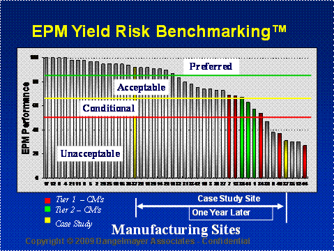
Figure 5: Industry EPM Yield Risk Benchmarking™
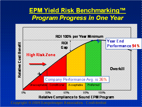
Figure 6: Industry EPM Yield Risk Benchmarking™
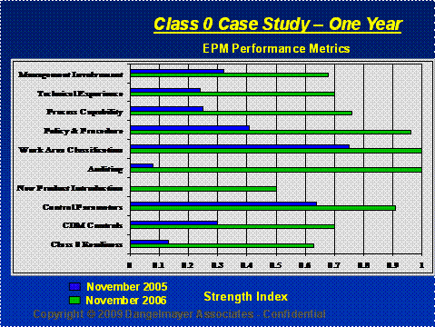
Figure 7: EPM Performance Metrics™
The analysis of the strengths and weaknesses of the ESD program are reflected in Figure 5 as well as the progress over one year. These indexes were derived from the EPM Yield Risk Benchmarking survey™ and were used as a guide for improvement. The data reflects substantial improvement to varying degrees. For instance, Auditing, New Product Introduction and Class 0 Readiness improved sharply during the year.
Auditing is one of the more critical elements of program management and, in this case, the improvement was essential to mitigate ESD losses. The data derived from this auditing plan was highly effective in the early identification and prioritization of process deviations. This data was also used to effectively leverage limited resources for better Class 0 compliance.
Below are two EPM improvement roadmaps (figure 6 and 7) that were used to track improvements. Figure 6 is the EPM Yield Risk Benchmarking™ and is a reflection of the ESD Quality System improvements. The blue line is the roadmap that was projected at the outset and the red line is the actual performance that was validated each month. Figure 7 is the closure timeline for the action items in the associated Technical Assessment.
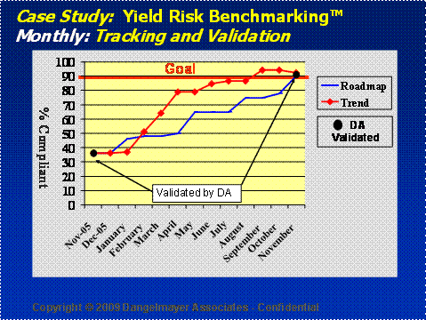
Figure 8: EPM Yield Risk Benchmarking™ Tracking Metrics
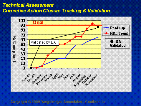
Figure 9: EPM Technical Assessment Findings Tracking Metrics
Class 0 Case Study #3: BAE Systems – Nashua, NH
Background:
This case study began during new product introductions when ESD failures were detected with failure analysis. BAE Systems had good ANSI/ESD S20.20 controls in place. However, even one failure would be too many for this high reliability application. So, prior to ramping up production, BAE Systems decided to bring in external expertise to prevent any production or reliability issues.
The approach of starting with a baseline Technical Assessment followed by customized reengineering of each critical operation, the use of quality tracking metrics and advance technical training was the same as Study #2. Naturally, the detailed process changes involved application appropriate customization and were significantly different.
EPM Yield Risk Benchmarking™ and ESD Quality Metrics:
BAE System’s Yield Risk Benchmarking™ score started at 53% and ultimately reached 94% (figure 10) and their process has not experienced even one ESD failure over a 3 year period since implementing the Class 0 controls. Virtually all elements of the EPM Performance metrics reach 90% or higher (figure 11). Both of the trend tracking metrics (Figures 12; 13 ) followed the roadmaps remarkably closely with impressive final scores of 93.6% and 96.6%. Figure 14 illustrates the remarkable improvement relative to the electronics and defense manufacturing industries.
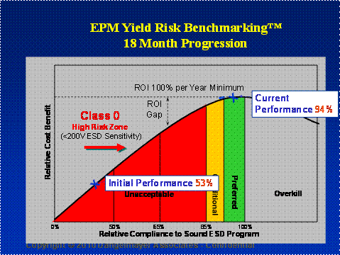
Figure 10: Industry EPM Yield Risk Benchmarking™
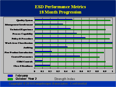
Figure 11: EPM Performance Metrics™
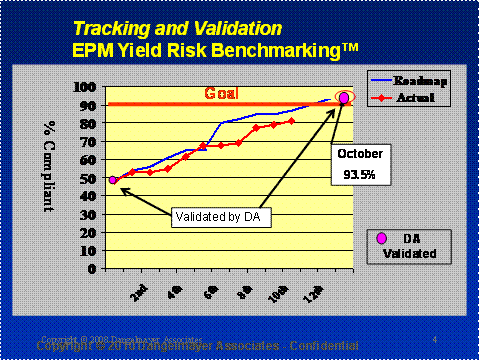
Figure 12: EPM Yield Risk Benchmarking™ Tracking Metrics
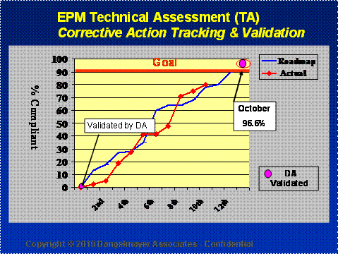
Figure 13: EPM Technical Assessment Findings Tracking Metrics
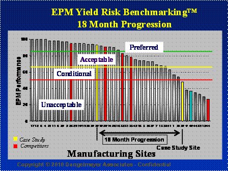
Figure 14: Industry EPM Yield Risk Benchmarking™
Conclusion:
The challenges presented by Class 0 ESD sensitivities are considerable and invariably require customization of mitigation techniques. The strategy used for these case studies employed the same basic elements and proved to be highly effective. ESD failures were virtually eliminated and the ESD team at each company became highly competent and well prepared for the next generation of more sensitive Class 0 devices.
- Administration of the program must be exceptional and include verification of the ESD performance of incoming new product designs.
- Quality metrics were also essential with tracking scores of over 90% in each category. If you cannot measure an ESD manufacturing process you do not have a functional process! With the process outlined here, you can successfully produce Class 0 products with very high yields.
- It is essential for both CDM and HBM counter measures to be executed with rigorous compliance verification and virtually flawless adherence to procedure to avoid quality or reliability excursions.
- In each case, a deep understanding of the ESD technology and Class 0 mitigation techniques were essential and were best learned through intense initial training with ongoing reinforcement over a year or more.
- CDM mitigation techniques must include both methods; minimizing voltages on the product and controlling the surface resistance of materials that contact the conductive elements of the ESDS product.
- Customized reengineering of critical operations was necessary and strategic application of dissipative materials and ionization.
- Advanced measurements such as ESD event detectors and current probes have become a critical element of Class 0 ESD programs.